

 Current location:home > News Center > Company News >
 2023-04-19


The first step of PCB process: cutting
Purpose of cutting: Cut large pieces of copper-clad sheets into small production boards of various required specifications.
Drilling process: confirm the plate thickness/copper thickness/size → cutting → grinding → grinding corners → washing the plate → baking the plate → next process
01 PCB cutting - copper clad laminate
First, let’s get to know the main raw material used in PCB - copper clad laminate.
Copper Clad Laminate (CCL for short) is a product made of wood pulp paper or glass fiber cloth as reinforcing materials, impregnated with resin, covered with copper foil on one or both sides, and hot pressed. It is called copper clad laminate.
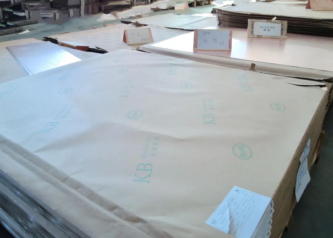
Copper clad laminate thickness
Commonly used copper clad laminate thicknesses are 0.3\0.5\0.7\0.9\1.1\1.5\1.9mm.
Note: The thickness of the copper clad laminate will increase by about 0.1mm during the production process.
Copper clad board size
1. Regular size
37*49 inches(940*1245 mm)
41*49 inches(1041*1245mm)
43*49 inches(1092*1245mm)
2.Customized size
1 inch = 25.4 mm
Copper Clad Laminate Brand
Xinjietongxin Circuit Board Factory focuses on industrial, communication module, and new energy industry customers, pursuing stability and reliability. We mainly use high-quality copper clad laminate brands (Shengyi, Jiantao).
02 PCB cutting - production board (Panel)
Due to the limitations of circuit board production equipment, we will divide the large copper clad laminate into several small boards. This division is called cutting. The small boards after being divided are processed on the production line and are called production boards (Panel).
How to determine the optimal processing size of the production panel?
This is the key to the PCB cutting process. Circuit board engineers need to design the best production board size to achieve maximum utilization of copper clad laminates and optimal production efficiency.
It mainly relies on the following two parts of the engineering department:
1. PCB panel design
Engineers use the finished board puzzle diagram (SET) provided by the customer to combine and layout, combine multiple SETs to form a panel (and production board), and then combine multiple panels to achieve the best utilization of the board.
Illustration of the relationship between Panel and SET:
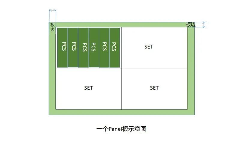
It means that one panel contains four SETs (each SET is the same), and one SET contains six PCS.
Jigsaw Puzzle File
The circuit board factory panel design is based on the customer's PCB file or Gerber source file. The PCB panel design drawing is completed according to the customer's needs, and the next step is to confirm that it is correct.
Board edge
Panels generally need to retain a certain edge to facilitate production in each step.
Generally, the default of circuit board factories is that the edge of double-sided panels is 8-10mm; the edge of multi-layer panels is 8-15mm; the actual edge of the board will be determined according to the size of the raw materials and the utilization rate of the panel.
The main purpose of puzzle
(1) Improve SMT production efficiency. Customers only need to do one SMT to complete the mounting of multiple PCB boards, thus improving welding efficiency.
(2) Improve cost utilization. Some PCBs are of special shapes. Reasonable panelization can improve the utilization rate of copper clad boards more efficiently and reduce cost waste.
2. Provide cutting drawings
The circuit board engineer determines the appropriate thickness, copper thickness and size of the copper clad laminate according to customer needs, and then cuts and divides it into blocks (taking 41*49 inches as an example) according to the panel design to form a cutting drawing.
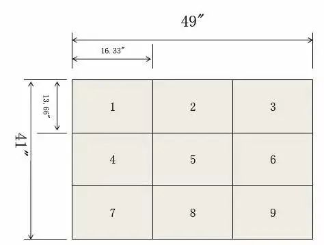
3*3 cutting diagram
03 PCB Cutting - Operation Process
With the cutting drawing, the production staff conducts the cutting operation of the copper clad sheet, which mainly includes the following three mechanical operation processes:
(1) Automatic cutting machine: Cuts large copper clad laminates into production boards of various sizes.
(2) Automatic edge grinding machine: Grinds the right-angle edges of the production board to make them smooth.
(3) Automatic corner rounding machine: rounds the corners of the board.
Note: It is very important to grind and deburr the edges to avoid unnecessary waste and pollution in subsequent processes.
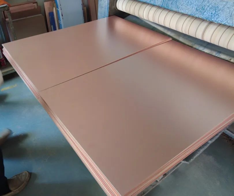
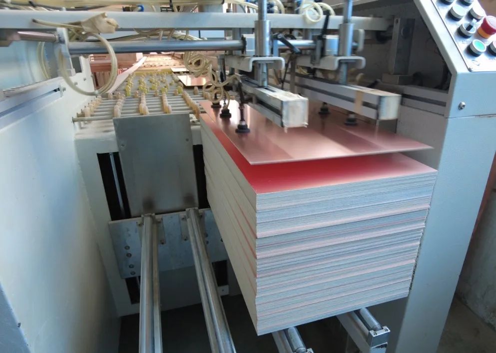
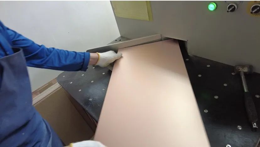
The production boards processed by the automatic cutting machine can only be transferred to the next process flow after washing and baking.
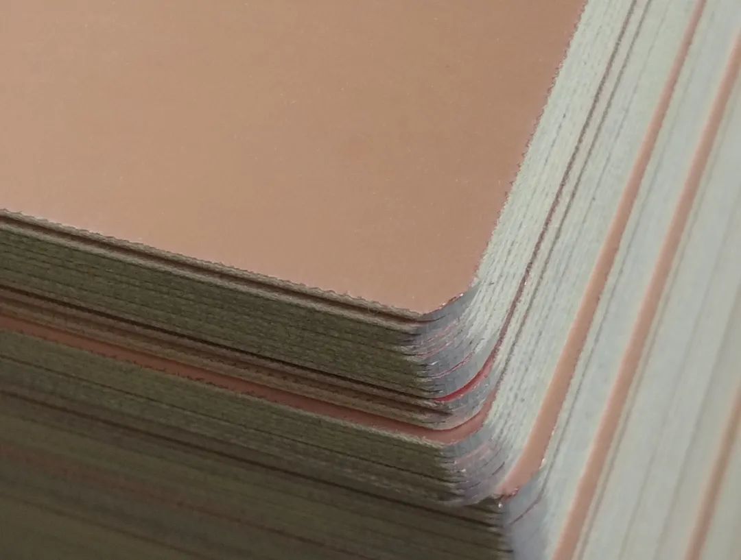
After the cutting process is completed, the sample board is produced (illustration)
Summary
Copper clad laminate is the main raw material of PCB. Due to different quality requirements, the cost price will be different. If the price of copper clad laminate is the same, the lower the utilization rate of the laminate, the higher the PCB price will be.