

 Current location:home > News Center > Company News >
 2023-04-19


Difficulty boards, half-hole boards, thick copper, and fine circuit boards are all covered!
PCB process flow four: circuit graphics
Process flow diagram:

Purpose:
After drilling and through-hole plating, the inner and outer layers have been connected. This process creates circuit patterns to achieve electrical integrity.
01 The whole process of graphic circuit production
1. Lamination
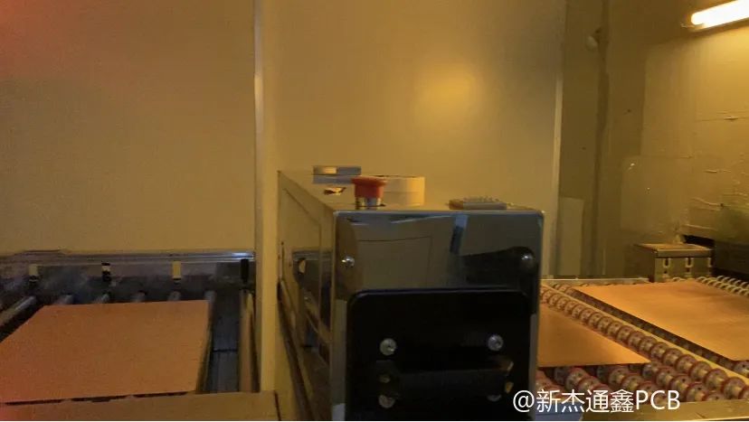
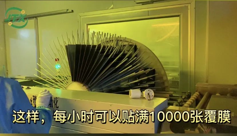
The treated copper surface of the substrate is pasted with a resist dry film through "hot pressing".
The automatic laminating equipment allows the substrate board to be controlled from entering the equipment to cooling, greatly improving the efficiency of laminating processing.
Basic diagram of lamination process:
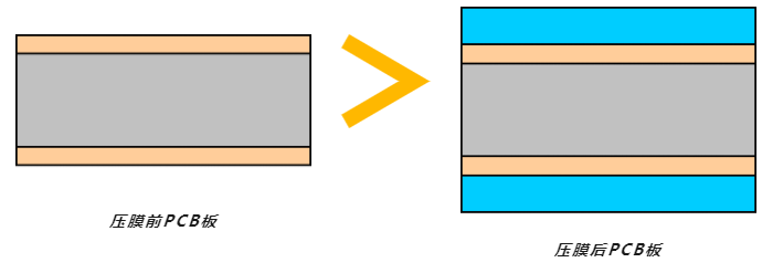
The blue layer is the dry film layer, which is actually only a thin layer.
2. Exposure process
On the LDI (laser direct imaging) exposure machine equipment, import the corresponding circuit pattern file, put in the substrate plate with the film pressed, perform exposure, and use laser light source energy to solidify the dry film in the pattern area.
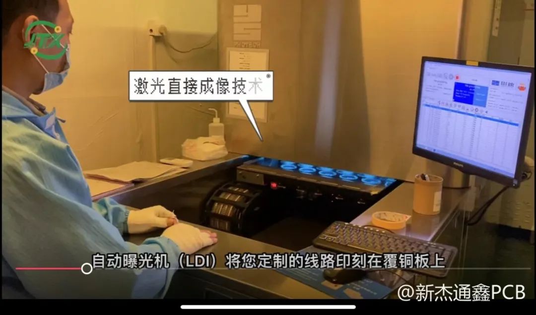
Basic diagram of the exposure process:
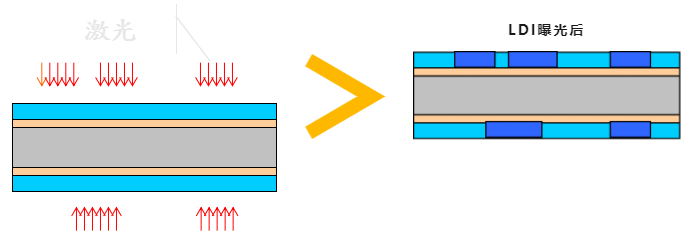
Precision circuit—"LDI exposure machine"
It uses laser scanning to directly image the image on the PCB, making the image more detailed and accurate.
In actual production, we use LDI exposure machines for high-precision exposure. For communication module boards and industrial boards that require high precision, the minimum line width and line spacing can meet 2.5 microns to meet the precision circuit design of PCB boards.
3. Development process
The uncured dry film is rinsed with a developer so that the image is clearly revealed on the board surface. The cured dry film will not be washed away by the developer and remains on the board surface as an anti-plating layer for electroplating or a protective layer for etching. .
Basic diagram of the development process:

02 Detection of graphic lines
In-group appearance line inspection will be carried out in every small link, and quality inspection will be carried out after the "line graphics" process is completed.
AOI inspection
The full name is Automatic Optical Inspection, automatic optical inspection.
Purpose:
The image is fed back to the device for processing through the principle of optical reflection, and compared with the set logical judgment principles or data graphics to find the location of the defect.
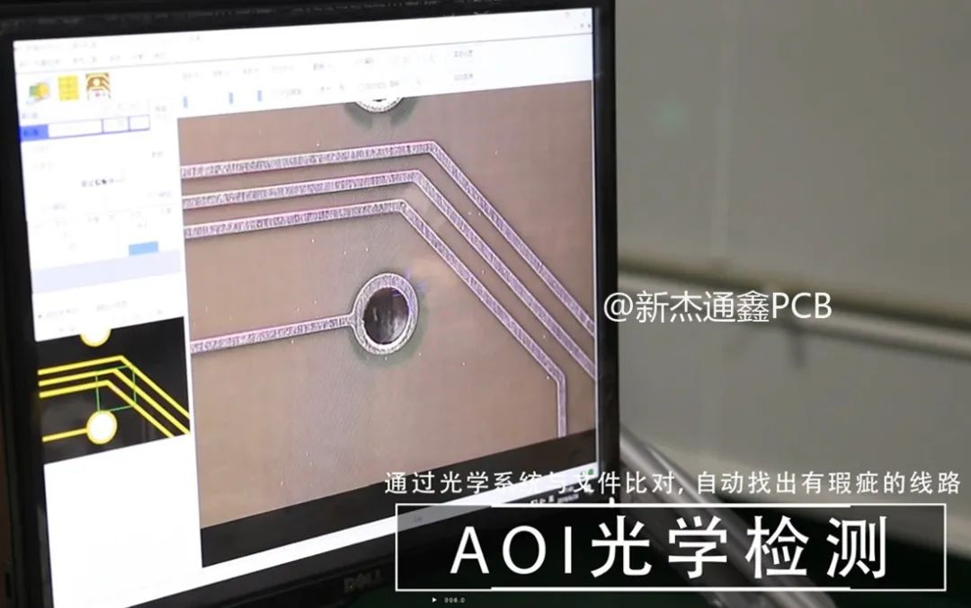
Defective products will be counted in batches and intercepted; only qualified products can enter the next process.