

 Current location:home > News Center > Company News >
 2023-04-19

Maybe we will be surprised that the base material of the circuit board only has copper foil on two sides, and there is an insulating layer in the middle. So how can the two sides or multi-layer circuits of the circuit board be connected together so that the current can pass smoothly?
Following the process of the previous article "PCB Process Flow 2: Drilling" (click to learn), the "copper sinking" process in this link will answer the above doubts.
PCB process flow three: Immersed copper PTH
Immersed copper is the abbreviation of Eletcroless Plating Copper, also called Plated Through hole, abbreviated as PTH.
The purpose of immersed copper is to chemically coat a thin layer of chemical copper on the non-conductive hole wall base material that has been drilled to prepare for the subsequent electro-copper and electro-tin in the "graphic electroplating" process and make it conductive. . After drilling the two-layer or multi-layer boards, the PTH process will be carried out.
Process flow:
Grind the plate before copper immersion → remove slag → water washing → alkaline degreasing → water washing → roughening (micro-etching) → water washing → pre-soaking → activation → water washing → acceleration → copper immersion → water washing → backlight detection → next process
01 PCB immersed copper - immersed copper front grinding plate
Immersed copper front grinding plate - clean the board surface
After the PCB substrate undergoes the pre-drilling process, burrs will inevitably occur, which is the most important hidden danger causing inferior hole metallization. Comprehensive cleaning must be done before copper sinking.
Before the PCB board enters the copper immersed wire, it will first pass through a plate grinder. The pre-copper plate grinder uses mechanical methods to initially clean the board surface and the inner hole wall.
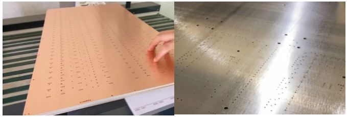
Observing the above comparison chart, we can see that the automatic plate grinding machine removes the dust attached to the plate surface and in the holes, as well as the residual batch front from the previous process, and removes oxidation to prepare for the next step of electroless copper deposition.
During the production process, PCB boards are exposed to the air for a long time and are easily oxidized, affecting the subsequent "copper" reaction.
02 PCB copper sinking-copper wire operation
Xinjie Tongxin PCB-Immersed Copper Wire
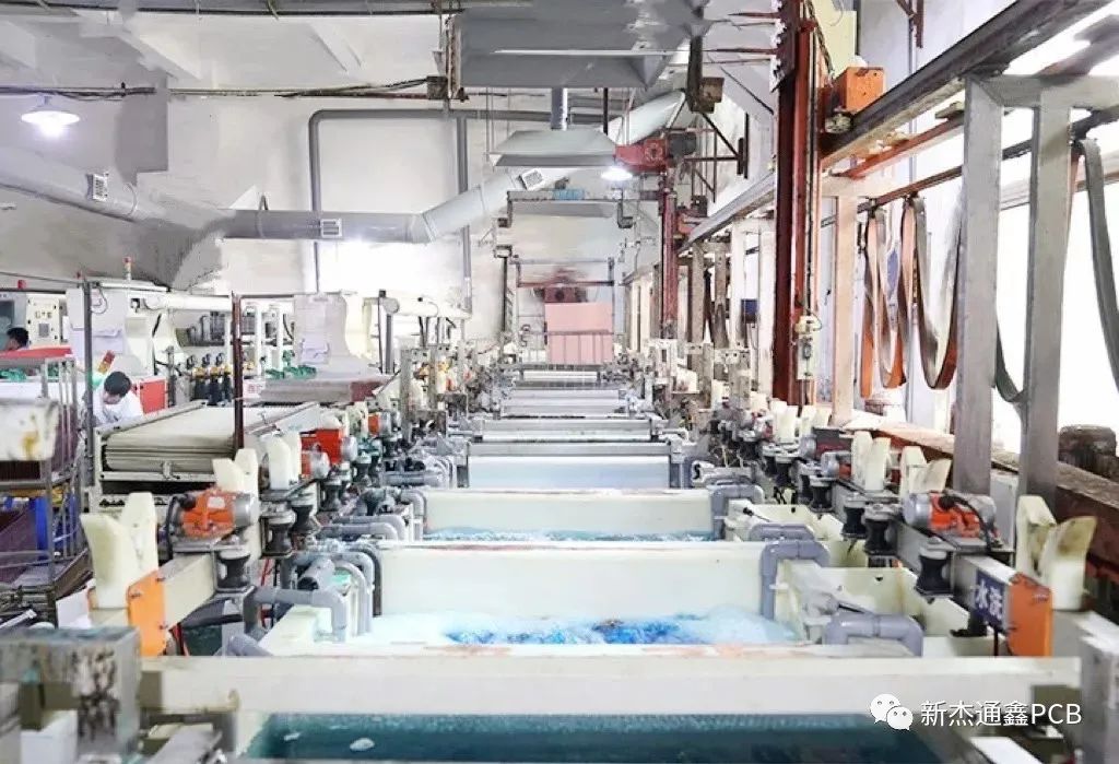
Xinjie Tongxin's automatic copper sinking wires perform different chemical reactions in sequence. The robotic arm picks up and places the boards. Professional department colleagues conduct real-time monitoring to ensure that the PCB board can successfully complete the copper sinking reaction.
The copper immersion wire mainly carries out the steps of removing slag → alkaline degreasing → roughening (micro-etching) → pre-soaking/activation → copper immersion, etc. Let’s learn more together.
1. Remove glue residue
Because the high temperature generated during drilling exceeds the glass transition temperature (Tg value), the resin softens and adheres to the hole wall as the drill bit rotates, producing slag.
Slag removal is to remove the slag attached to the hole wall during drilling and expose the copper rings that need to be interconnected on each layer.
Tg value: glass transition temperature. (This chapter will not be expanded upon)
Gum removal method
The reaction principle of potassium permanganate and epoxy resin
6KMnO₄+(C11H12O3)n =3K2MnO4+3MnO2+3CO2↑+3H2O
Under the action of KMnO4, the bond between the benzene ring and oxygen in the epoxy resin is broken, and then KMnO4 and the group generate K2MnO4, CO2, and H2O.
That is, after the above reaction, the epoxy resin is removed.
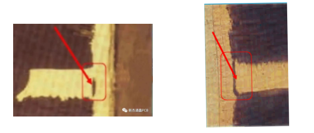
If the slag is not removed completely, a gap that cannot be connected will be left between the copper hole wall and the inner hole ring, causing an open circuit. See diagram below:
2. Alkaline degreasing
Remove oil stains, fingerprints, and oxides from the board surface; adjust the polarity of the pore wall base material (adjust the pore wall from negative charge to positive charge) to facilitate the adsorption of colloidal palladium (activator) in the subsequent process.
The quality of the oil removal adjustment directly affects the effect of the immersed copper backlight.
3. Micro corrosion
Remove oxides from the board surface and roughen the board surface to ensure good bonding between the subsequent copper deposited layer and the base copper of the substrate; the newly generated copper surface is highly active and can well absorb colloidal palladium.
4. Pre-soaking/activation treatment
Pre-soaking : protects the palladium tank from contamination of the pre-treatment tank liquid and facilitates the effective activation of subsequent activation liquid.
Activation : After adjusting the polarity of alkaline degreasing in pre-treatment, the positively charged pore walls can effectively absorb enough negatively charged colloidal palladium particles to ensure the uniformity, continuity and density of subsequent copper deposition.
Oil removal and activation play a very important role in the quality of subsequent copper deposition. Therefore, special attention should be paid to the activation effect during production, ensuring sufficient time, concentration (or intensity), and temperature are all indispensable.
5. Copper immersion (chemical copper immersion):
The activation of the palladium tank induces an autocatalytic reaction of electroless copper deposition . The newly generated chemical copper and the reaction by-product hydrogen can be used as reaction catalysts to catalyze the reaction, so that the copper deposition reaction continues.
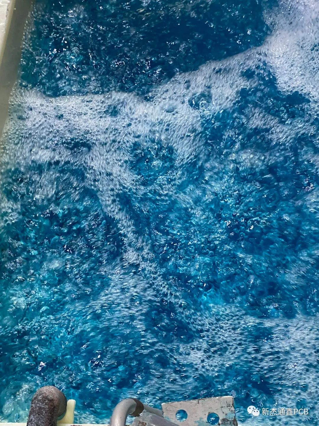
Immersed copper trough
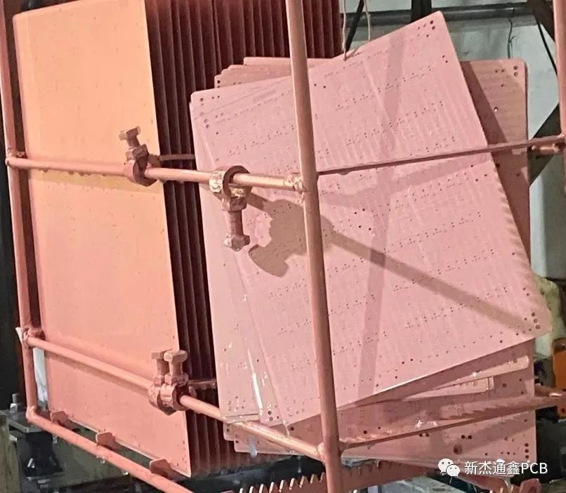
After following the copper immersion wire operation steps, a layer of chemical copper can be deposited on the board surface or hole wall.
The thickness of the deposited copper formed is generally very thin, usually only 0.3~0.5μm. With the change of chemical solution, the copper thickness of the deposited copper process can be about 2μm.
03 PCB copper sinking—backlight inspection
After the copper deposition process is completed, all circuit boards need to be quality tested one by one: mainly backlight testing is used to check the copper deposition coverage and coverage integrity.
The effect of immersed copper will directly affect the overall product quality of the circuit board, because once a quality problem occurs, it is often a problem with the entire batch, not a single panel. Therefore, when performing this production process, operating specifications must be strictly followed to prevent irreversible quality hazards to the product.
Production sampling
According to the production batch, slice the 5 holes on the edge of the circuit board after copper immersion as a copper immersion sample for observation.
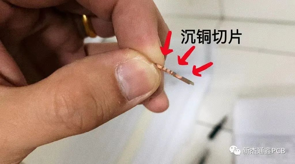
Backlight inspection
Use a magnifying glass to perform backlight inspection in the laboratory to evaluate and monitor the deposition coverage of plated through holes in the PTH process (PTHprocess)
Backlight inspection standard chart
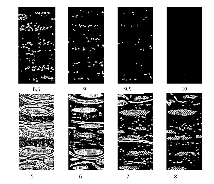
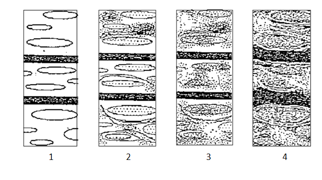
quality assessment
Generally, circuit board manufacturers use grades greater than or equal to 9/9.5 as the dividing point to be judged as qualified. Our company's backlight level requirement is greater than or equal to 9.5 to be considered qualified, and unqualified products need to be reworked twice.
The evaluation and monitoring of the deposition coverage of plated through holes in the PTH process (PTHprocess) is a very important quality control check.
This ensures that the plating layer after chemical copper deposition can effectively provide the conductivity and other performance requirements for subsequent plated through holes, and can also promptly detect some unpredictable problems in the production line and perform necessary or possible rework in this process in a timely manner.
The circuit board industry needs to pay attention to quality supervision in every link to ensure the perfect delivery of the final product.