• Home
  • About Us
    Company Introduction
    Honorary Qualifications
    Corporate Culture
    Development History
    Factory Showcase
  • Product Center
    Security
    Industrial
    Communications
    Consumer
    Special Materials
  • Technical Parameters
    Process Capabilities
    Delivery Capabilities
    Inspection Standards
  • News Center
    Company News
    Industry News
    FAQ
  • Contact Us
    Contact Us
    Online Recruitment
CN
  • home
  • About Us
    Company Introduction
    Honorary Qualifications
    Corporate Culture
    Development History
    Factory Showcase
  • Product Center
    Security
    Industrial
    Communications
    Consumer
    Special Materials
  • Technical Parameters
    Process Capabilities
    Delivery Capabilities
    Inspection Standards
  • News Center
    Company News
    Industry News
    FAQ
  • Contact Us
    Contact Us
    Online Recruitment
  • Company News
  • Industry News
  • FAQ
  • Current location:home > News Center > Company News >
  • [PCB Process] Process 4: Illustrated explanation of "circuit graphics"! Key chapters must read

    [PCB Process] Process 4: Illustrated explanation of "circuit graphics"! Key chapters must read

    Difficulty boards, half-hole boards, thick copper, and fine circuit boards are all covered!PCB process flow four: circuit graphicsProcess flow diagram:Purpose:After drilling and through-hole plating, the inner and outer layers have been connected. This process creates circuit patterns to achieve ele
    2023-04-19
  • [PCB Process] Process 3: The copper-immersion PTH production process is exposed, highlight the key points!

    [PCB Process] Process 3: The copper-immersion PTH production process is exposed, highlight the key points!

    Maybe we will be surprised that the base material of the circuit board only has copper foil on two sides, and there is an insulating layer in the middle. So how can the two sides or multi-layer circuits of the circuit board be connected together so that the current can pass smoothly?Following the pr
    2023-04-19
  • [PCB Process] Step 2 of the process: Is there a lot to learn about small holes? High-definition drilling pictures!

    [PCB Process] Step 2 of the process: Is there a lot to learn about small holes? High-definition drilling pictures!

    PCB process flow 2: drillingIn the previous article, we introduced the PCB cutting process (click to learn more). This part comes to the PCB drilling process.PCB drilling: Drill holes on the board surface according to routing or structural requirements.Drilling process:Double sided board drillingCut
    2023-04-19
  • [PCB Process] The first step of the process: What are the details of cutting that you don’t know? Useful information!

    [PCB Process] The first step of the process: What are the details of cutting that you don’t know? Useful information!

    The first step of PCB process: cuttingPurpose of cutting: Cut large pieces of copper-clad sheets into small production boards of various required specifications.Drilling process: confirm the plate thickness/copper thickness/size → cutting → grinding → grinding corners → washing the plate → baking th
    2023-04-19
  • The spring breeze is blowing vigorously, and we are setting sail for glory - warm congratulations to the park-Chongqing Jietongxin Electronics Co., Ltd., the company that has entered the park, for its successful commissioning ceremony!

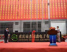
    The spring breeze is blowing vigorously, and we are setting sail for glory - warm congratulations to the park-Chongqing Jietongxin Electronics Co., Ltd., the company that has entered the park, for its successful commissioning ceremony!

    The spring breeze is strong and the Year of the Rabbit is auspicious. In this spring of sowing and nurturing hope, everything is revived and full of spring. Chongqing Electronic Circuit Industrial Park ushered in another major event. At 10:10 am on March 10, 2023, Chongqing Electronic Circuit Indust
    2023-03-10
    • <
    • 1
    • 2
    • >

About Us

  • Company Introduction
  • Honorary Qualifications
  • Corporate Culture
  • Development History
  • Factory Showcase

Product Center

  • Security
  • Industrial
  • Communications
  • Consumer
  • Special Materials

Technical Parameters

  • Process Capabilities
  • Delivery Capabilities
  • Inspection Standards

News Center

  • Company News
  • Industry News
  • FAQ

Contact Us

  • Contact Us
  • Online Recruitment

Contact Details

  • Market Department 117727819952
  • Marketing Department 213048827666

Friendly Links

  • 2-layer circuit board
  • Order hotline:17727819952
    Shenzhen Office Address:Room 405, Building B, Xinbaoyi Industry and Trade Building, Houting Community, Shajing Street, Baoan District, Shenzhen
    Chongqing Factory Address:Building 10, Zone B, Electronic Circuit Industrial Park, Rongchang District, Chongqing
Copyright @ 2019 Shenzhen Xinjietongxin Electronics Co., Ltd. All Rights ReservedNanbo.com粤ICP备15107872号

About Us

Company Introduction
Honorary Qualifications
Corporate Culture
Development History
Factory Showcase

Product Center

Security
Industrial
Communications
Consumer
Special Materials

Technical Parameters

Process Capabilities
Delivery Capabilities
Inspection Standards

News Center

Company News
Industry News
FAQ

Contact Us

Contact Us
Online Recruitment

Contact Details

Market Department 117727819952
Marketing Department 213048827666

Friendly Links

  • 2-layer circuit board
  • Contact Us

    Order hotline:17727819952
    address:Room 405, Building B, Xinbaoyi Industry and Trade Building, Houting Community, Shajing Street, Baoan District, Shenzhen
    Copyright @ 2019 Shenzhen Xinjietongxin Electronics Co., Ltd. All Rights ReservedNanbo.com    Guangdong ICP No. 15107872